需要我們的協助嗎?

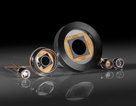
Silicon Photodiodes
Through the photovoltaic effect, detectors provide a means of transforming light energy to an electrical current. The root of the theory behind this phenomenon is a small energy gap between the valence and conduction bands of the detector. When light, with enough energy to excite an electron from the valence to the conduction band, is incident upon the detector, the resulting accumulation of charge leads to a flow of current in an external circuit. Since light is not the only source of energy that can excite an electron, detectors will have some amount of current that is not representative of incident light. For example, fluctuations in thermal energy can easily be mistaken for light intensity changes. A variety of these “non-light” contributions are present and, when summed up, make up the total noise within the detector.
The ratio of the overall signal output to the noise level is known as the signal to noise ratio (s/n) and can be used to determine if noise will be a concern within a particular application. While noise is certainly a key means of characterizing detectors, it is only one of the characteristics which should be considered when selecting a detector.
Photovoltaic (Unbiased): During PV operation, no external bias is applied to the photodiode. Since Dark Current is a function of bias magnitude, PV operation eliminates Dark Current as a source of noise. In this case, the NEP will be lower, thereby allowing greater sensitivity at lower wavelengths. This makes it ideal for low signal detection. One disadvantage is the slightly lower responsivity at higher wavelengths (see graph).
Photoconductive (Biased): During PC operation, a reverse bias on the photodiode results in a number of response advantages, such as a faster rise time. This makes this type of operation more suitable for high frequency applications. One inconvenience is that the dark current increases with this applied biased current, so noise is introduced into the system.


or view regional numbers
QUOTE TOOL
enter stock numbers to begin
Copyright 2023, Edmund Optics Inc., 14F., No.83, Sec. 4, Wenxin Road, Beitun District , Taichung City 406, Taiwan (R.O.C.)
Privacy Policy | Cookie Policy | Terms & Conditions | Accessibility
California Consumer Privacy Act (CCPA): Do Not Sell My Information
The FUTURE Depends On Optics®